
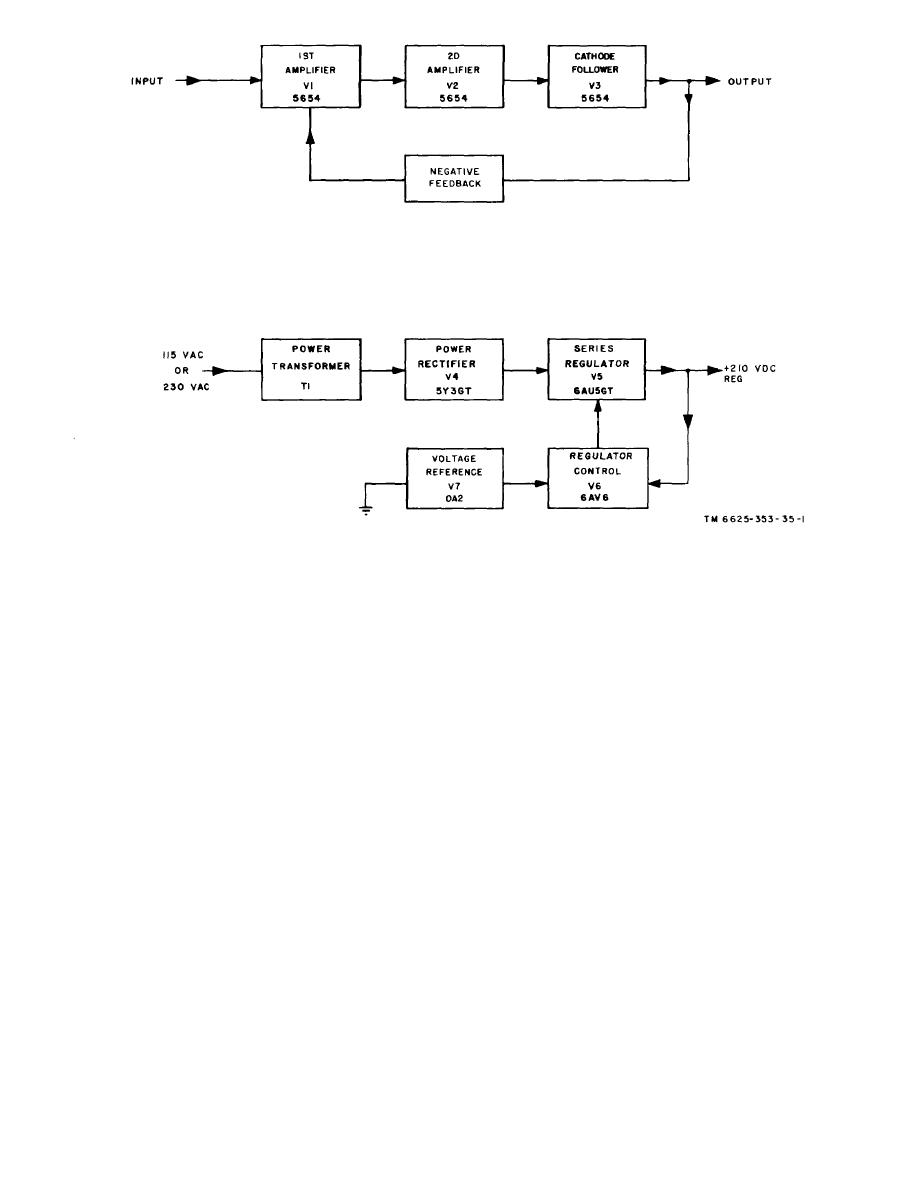
Figure 1. Amplifier, Radio Frequency AM1881/U,
block diagram.
hf response. Resistor R8 reduces the volt-
present in the signal applied to the INPUT
age applied to the V1 screen; C2A bypasses
terminal. Resistor R1 provides the grid
with a ground return path, while R2 is a
the screen to ground. Resistor R9 is the
parasitic suppressor. Resistor R3A with
plate load resistor; R10, with C2B and
R3B and R3C is a tapped, wire-wound
C 2 C , decouples V1 from V2 and V3.
resistor that forms a voltage divider net-
Capacitor C3 couples the amplified signal
work (together with R6) for the feedback
to the grid of V2.
signal. Resistor R3Bprovides cathode bias
b. Second Amplifier. The second am-
for V1 and the required level of degnera-
plifier, V 2 , functions the same as V1
tion for a total overall rf amplifier gain
except that no feedback signal is intro-
of 40 decibels (db) when GAIN switch S1 is
duced into V2.
set to 40 DB. Resistor R3A provides the
c. Cathode Follower. Cathode follower
degeneration required for a total gain of
V3 is a type-5654 pentode connected as a
20 db when the GAIN switch is set to 20
t r i o d e cathode follower. Resistor R29
DB. Resistor R6 permits adjustment of the
provides cathode bias for V3 as well as
negative feedback for Vl; R18 is the cath-
negative feedback over a small range to
ode load resistor. Capacitor C6 couples
calibrate the rf amplifier gain. Capacitor
Cll adjusts the amount of feedback and is
the amplified signal to the OUTPUT ter-
minal and blocks the dc component. Re-
used to adjust the rf amplifier frequency
sistor R19 provides a ground return path
response between 1 and 2 mc. Capacitor
for the negative side of C6 and the OUT-
C 1 2 reduces degeneration at high fre-
PUT terminal.
quency (hf) and is selected to give a flat
3
