TM 11-5821-333-30
3-3. PROCESSOR MODULE
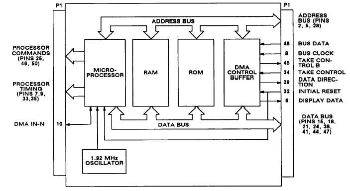
Figure 3-3 is a block diagram of the processor module. The processor module has a clock, microprocessor,
RAM, ROM, and DMA control buffer. The functions of the microprocessor are to
l read and execute instructions stored in memory,
l control input/output devices,
l transfer data between input/output devices and memory,
l transfer data between memory locations.
The functions of the DMA control buffer are to
l receive serial data from the rt via the bus interface module and make the data available to the
microprocessor on the data bus,
l receive TAKE CONTROL input from external take control input and inform microprocessor,
l perform parallel to serial data conversion for data going from microprocessor to front panel display,
l buffers DATA DIRECTION output.
Data transfers that do not go through the DMA control buffer are control data to rt (output), rotary switch data
(input), and pushbutton switch data (input). Rt control data is sent to the bus interface module via the data bus.
Rotarv switch data is received from the front panel via the data bus. Pushbutton switch data is received from the
keyboard encoder on the bus interface module via the data bus.
Figure 3-3. Processor Module Functional Block Diagram
3-4. POWER SUPPLY MODULE
Figure 3-4 is a block diagram of the power supply module.
The protection circuit has +28 V dc filtering. It attenuates spikes and surges per MIL-STD-704B. It also protects
against reverse voltage and over voltage. The pulse width modulator is a constant frequency, variable
pulse-width circuit. It regulates output voltage by varying pulse width to the de-de converter. The de-de converter
chops the +28 V dc. The resulting square wave is rectified, filtered, and regulated to the required output volt-
ages: +5 V dc and -22 V dc. Current limiters protect the power supply in case of thermal runaway caused by
overheating. Also they limit output current if a short circuit is applied. A low-voltage reset circuit monitors the
3-4


